Printed circuit boards (PCBs) are at the core of practically all modern electronic devices. They feature electrical components connected by engraved conductive pathways, which enable them to serve as a more compact and easy-to-install alternative to traditional multi-wire circuits. As they are highly customizable, industry professionals can tailor them to meet their needs, whether they require rigid, flexible, or rigid-flex designs and one or multiple layers.
While this customizability allows PCBs to accommodate the requirements and restrictions of a wide range of electronic applications, it also makes it more challenging to determine the ideal printed circuit board design and assembly configuration. Partnering with an experienced PCB supplier, such as Redstar Worldwide, can streamline both the selection and sourcing process by helping to assess what design specifications are necessary and connect with reputable PCB manufacturers.
Below we cover the following topics to acquaint you with basics of PCB and why Redstar Worldwide is an ideal partner for all PCB needs:
- What is a PCB?
- Important PCB Terminology
- Typical PCB Materials
- Types of PCBs
- Applications of PCBs
- PCB Capabilities at Redstar
- Why Choose Redstar Worldwide?
A Basic Overview of Printed Circuit Boards
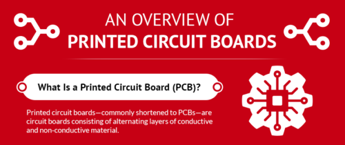
What Is a Printed Circuit Board (PCB)?
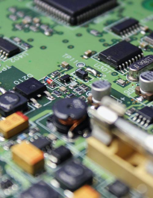
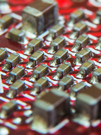
Printed circuit boards—commonly shortened to PCBs—are circuit boards consisting of alternating layers of conductive and non-conductive material. The inner conductive layers feature copper etchings that allow power and signals to pass to connected circuit components. Once the etchings on a layer are complete, the layer is laminated with insulating material. This process is repeated until the PCB is fully constructed.
Depending on the intended use case, the design may feature one to 20 or more layers. After all etching and lamination stages, electrical components are added to the board, either through surface mount or through-hole methods, and soldered in place. The finished assembly is then plated, coated with solder mask, and silk screened with any necessary information.
Important PCB Terminology
When selecting and sourcing PCBs, several technical terms may be encountered, such as:
- Finger: exposed metal along the edge of the PCB that forms connections between two separated boards
- Pad: exposed metal on the surface of the PCB on which electronic components are soldered
- Silk screening: a printing process used to add letters, numbers, symbols, and other important information to the surface of the PCB
- Slot: a non-circular hole in the PCB
- Solder mask: protective material added to a finished PCB that prevents short circuiting, corrosion, and other common electronic problems
- Surface mount technology: a mounting method that employs the use of holes as a connection or mounting point for electronic components
- Through-hole technology: a mounting method that allows electronic components to be placed directly on the board without the need for holes
- Trace: the continuous pathways of copper on a PCB that connect electronic components
Typical PCB Materials
Each of the layers of a PCB—the base material, the conductive pathways, the solder mask, and the silk screen—employ different materials.
- The base material, also referred to as the substrate, can be rigid or flexible, depending on the PCB design. Manufacturers often use fiberglass (e.g., FR4) for rigid sections and high-temperature flexible plastics (e.g., polyimide or PEEK) for flexible sections.
- The conductive pathways are made from copper and are laminated to one or both sides of the substrate, depending on PCB design.
- The solder mask is an insulating material that covers the substrate and conductive pathways to protect against incidental contact with other conductors. While it is generally green, it is available in additional colors, such as red, white, and purple.
- The silk screen design sits on top of the solder mask layer, indicating assembly and use instructions for users. While white inks are most common, other colors are also employed, including black, gray, red, and yellow.
Types of PCBs
PCBs are available in several design variations to suit different applications. The main types available are:
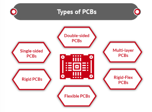
- Single-sided PCBs: also referred to as single-layer PCBs—contain only one conductive layer and, therefore, only one side on which to mount electrical components. While inexpensive, they are rarely used in industrial devices. Typical applications include calculators, printers, and radios.
- Double-sided PCBs: also known as double-layer PCBs—have conductive elements on both sides of the board. Through-holes can be used to connect the components on opposing sides.
- Multi-layer PCBs: Multi-layer PCBs have three or more conductive layers. They are generally used in highly complex electronic applications, such as data storage, GPS systems, and medical devices.
- Rigid PCBs: Rigid PCBs are constructed with inflexible materials, such as fiberglass, to prevent twisting. They are available in single-sided, double-sided, and multi-layer designs.
- Flexible PCBs: Flexible PCBs are printed on a flexible substrate to allow them to fit into small or irregular enclosures. They are available in static-flex or dynamic-flex designs. Static-flex PCBs are designed to remain in a given position once installed, while dynamic-flex PCBs are designed to withstand repeated bending without failure.
- Rigid-Flex PCBs: Rigid-flex PCBs combine the advantageous characteristics of rigid and flexible PCBs, consisting of rigid sections connected by flexible segments.
Applications of PCBs
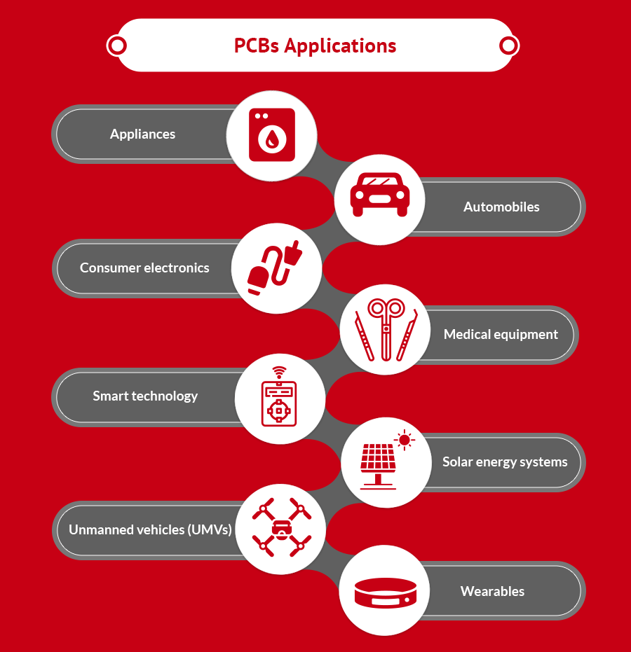
Due to their superiority in performance compared to traditional circuits, PCBs find application in many electronic devices, equipment, and systems, including, but not limited to, the following:
- Appliances
- Automobiles
- Consumer electronics
- Medical equipment
- Smart technology
- Solar energy systems
- Unmanned vehicles (UMVs)
- Wearables
Sourcing PCBs With Redstar Worldwide
At Redstar Worldwide, our relationships with reputable overseas manufacturers allow us to deliver high-quality PCB solutions at competitive prices. We offer the following PCB capabilities:
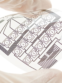 . Flexible & Rigid-Flex PCB Solutions
Flexible PCBs are built with a flexible substrate that allows the board to bend for use in limited-space environments or products designed to flex. They are used in many electronic devices, such as:
- Computer systems (e.g., data storage and servers)
- Consumer electronics (e.g., cell phones and digital cameras)
- Green energy systems (e.g., solar)
- Internet of Things (IoT) systems
- Medical equipment
- Military and defense systems
- Smart glass
- Testing equipment
- Tools
- Wearable technology and biometric devices
Rigid-Flex PCBs have both flexible and rigid components that allow them to fold or flex in certain configurations but remain solid and stable in others. They often find application in the following:
- Automobiles
- Cell phones
- Green and solar energy
- Internet of Things (IoT) systems
- Medical equipment
- Tools
- Wearable devices
 . Metal Core Printed Circuit Board Solutions
Metal core PCBs are ideal for situations in which thermal management is a chief concern. Smaller traditional PCBs do little to prevent overheating, which can pose a problem at high processing speeds. Metal core PCBs are printed onto a base metal with a dielectric polymer layer, which facilitates heat dissipation to allow for consistent performance.
 . HDI Technology Solutions
High-density interconnect (HDI) PCBs are designed to pack more circuitry into a board of the same size by decreasing the size of components and optimizing the placement of board elements. The end result is faster, more efficient processing capabilities in a more compact package.
 . Quick Turn Prototyping Solutions
We offer quick-turn prototyping services for all PCB varieties. Turnarounds for standard FR4 or double-sided PCBs are as low as 24 hours, while more complex designs require 5–10 days. We begin a manufacturability review within hours of receiving files and carry out comprehensive quality checks throughout the process to ensure that the finished prototype functions as intended.
. PCB Engineering Solutions
We employ expert field application engineers to guide clients through the design process. When consulting with clients, they focus on common pain points that can drive prices up and efficiency down. These services are available for all of our PCB offerings and ensure that each client receives quality products without exceeding their budgets.
Why Choose Redstar Worldwide?
At Redstar Worldwide, we are committed to ensuring the PCB needs of our clients are fully met. Equipped with decades of experience, our team has the knowledge and skills to help identify and source the ideal PCB design for a given application. To learn more about our PCB capabilities, contact us or request a quote today.